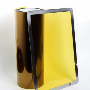
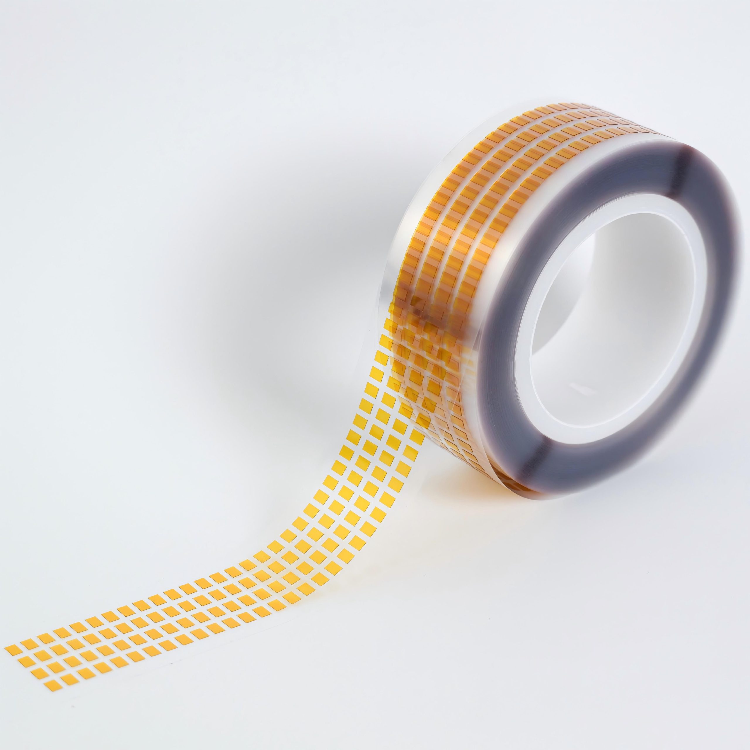
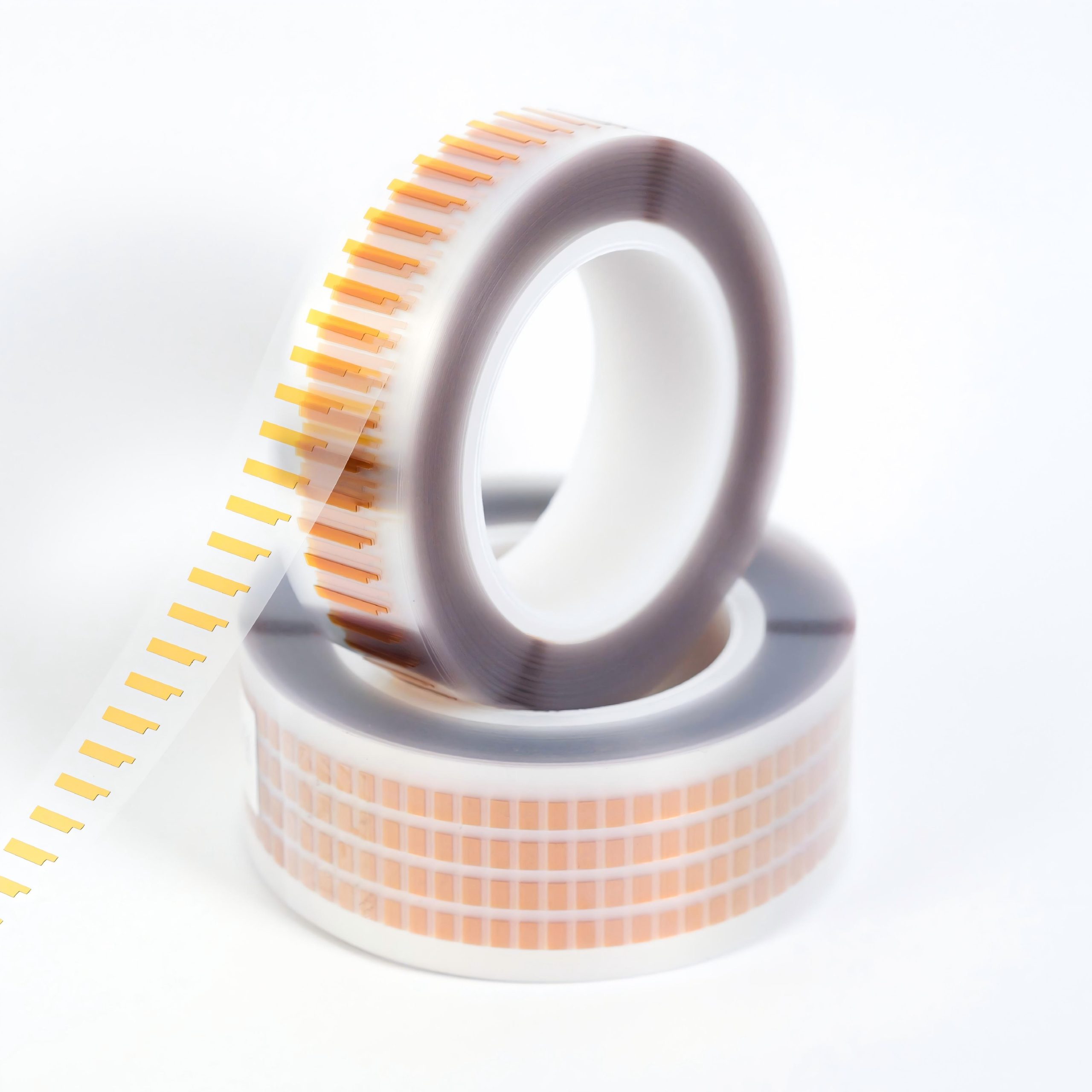
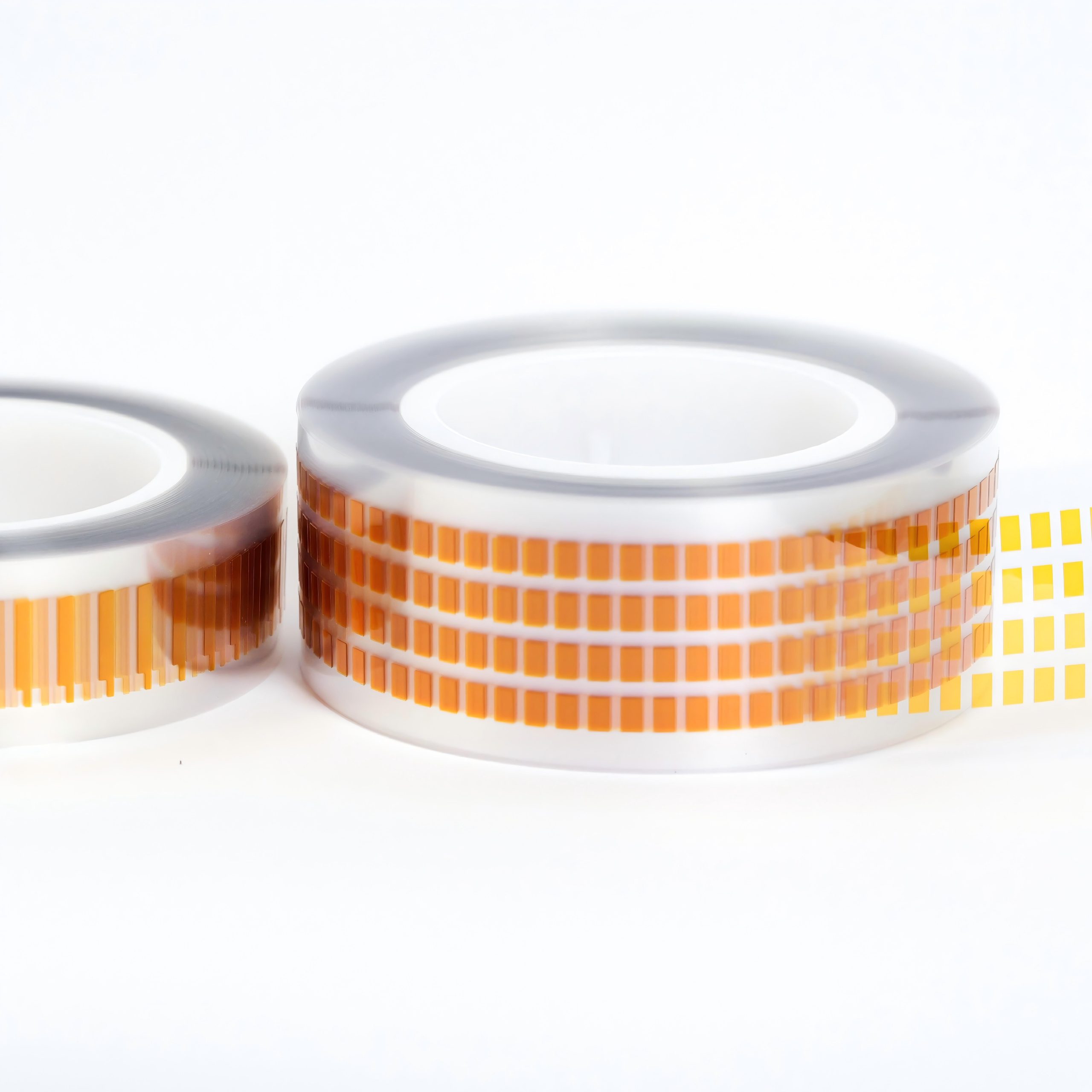
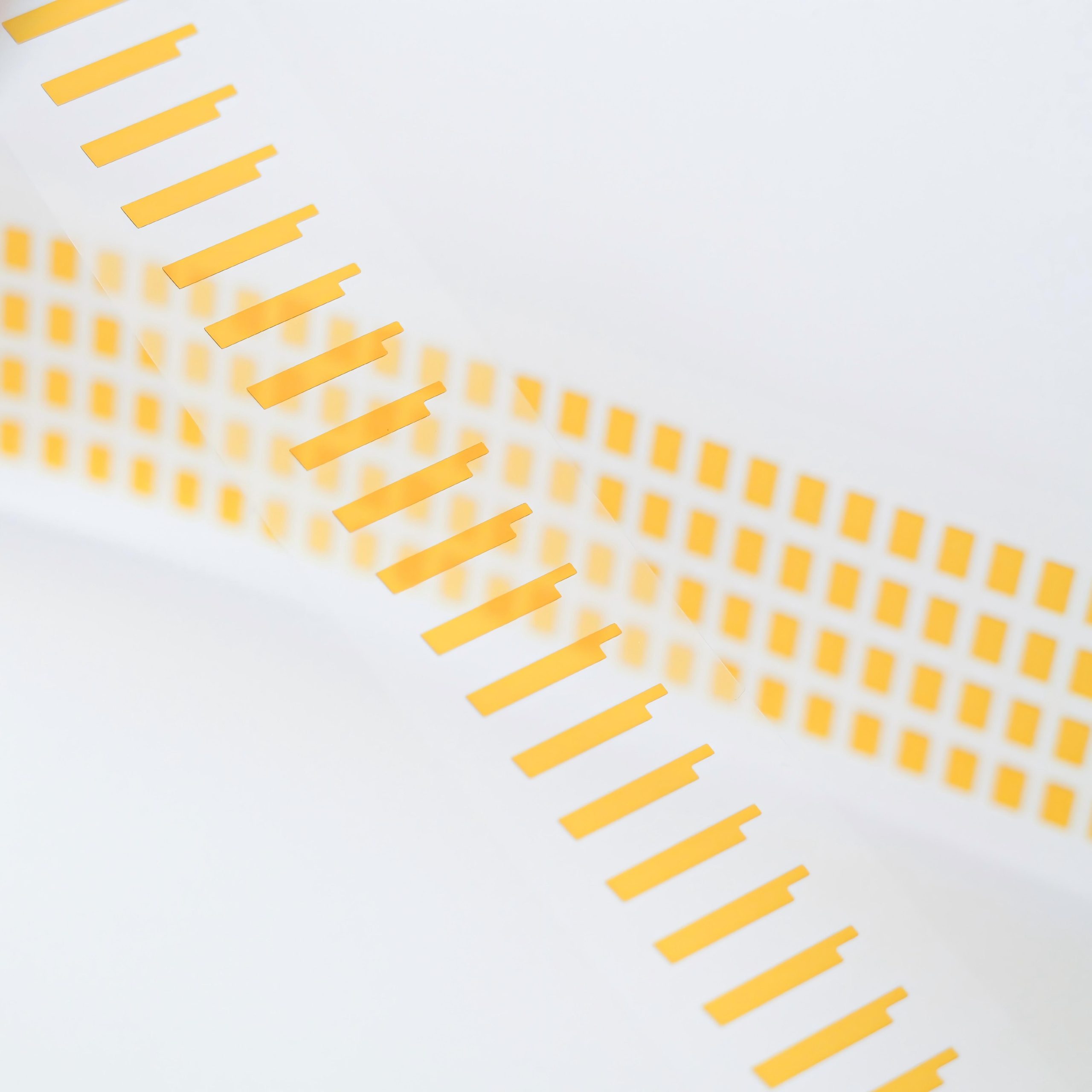
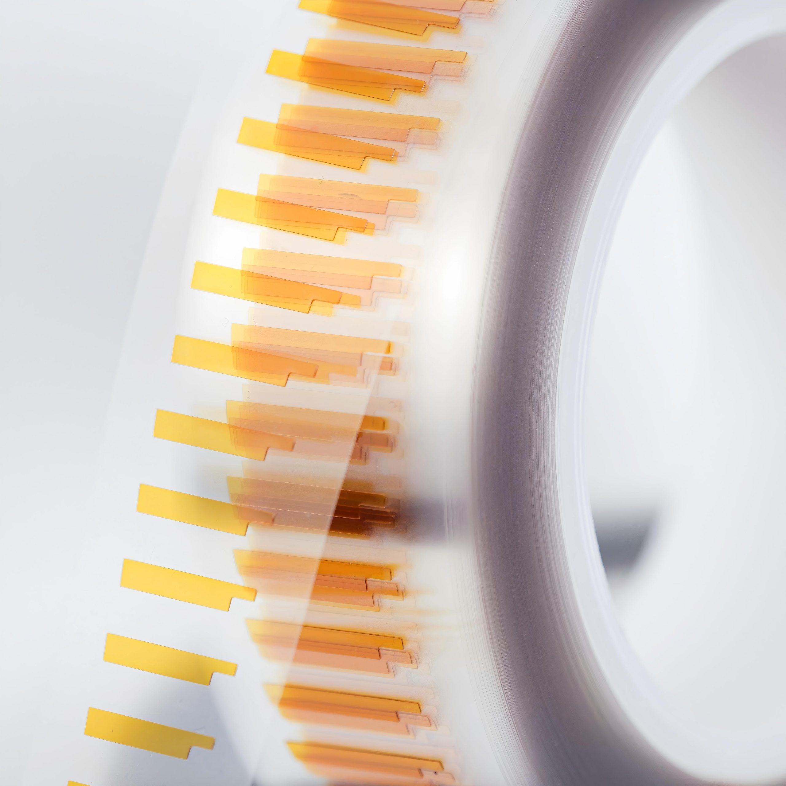
ESTEE Masking Tape is a custom die-cut process material applied to designated areas of the semiconductor package that must remain free of metal deposition. Unmasked areas remain exposed during sputtering, creating the required selective EMI shielding coating.
The solution is particularly suitable for double-sided molded packages, as well as packages with solder balls, bumps, components or stepped topography.
Material construction, adhesive performance and die-cut geometry are engineered around the package drawing, mask/deposition boundary, surface topography, equipment interface and sputtering conditions.
Key Performance
|
Parameter |
Typical Value |
|
ESD performance |
Surface resistance: 104-10⁹ Ω/sq |
|
Temperature condition |
<260°C for 30 min |
|
Process cleanliness |
Designed for low residue, overflow and burr |
|
Automation compatibility |
Custom die-cut format for automated front-side placement |
Representative Models
|
Tape Model |
Total Thickness (μm) |
Base Film Thickness (μm) |
Adhesive Thickness (μm) |
180° Peel Adhesion (gf/inch) |
|
SP-CR-165PI150L |
165 |
75 |
90 |
150 |
|
SP-CR-125PI250L |
125 |
50 |
75 |
250 |
|
SP-CR-55PI250L |
55 |
25 |
30 |
250 |
|
SP-CR-130PI280L |
130 |
50 |
80 |
280 |
Function in Selective EMI Sputtering
|
Process Requirement |
Function of the Masking Tape |
|
Local masking |
Protects designated functional regions that must remain unmetalized. |
|
Mask/exposure boundary |
Custom outlines, openings and reliefs define where metal deposition is blocked or permitted. |
|
Feature accommodation |
Reliefs and conformable profiles are designed to accommodate solder balls, bumps, copper pillars, components and steps. |
|
Boundary stability |
Helps control edge lifting, local gaps and overflow beyond the intended deposition boundary during vacuum and sputtering. |
|
Controlled removal |
Supports removal after sputtering while minimizing residue, burr and stress on package features. |
Key Performance
|
Parameter |
Typical Value |
|
ESD performance |
Surface resistance: 104-10⁹ Ω/sq |
|
Temperature condition |
<260°C for 30 min |
|
Process cleanliness |
Designed for low residue, overflow and burr |
|
Automation compatibility |
Custom die-cut format for automated front-side placement |
Representative Models
|
Tape Model |
Total Thickness (μm) |
Base Film Thickness (μm) |
Adhesive Thickness (μm) |
180° Peel Adhesion (gf/inch) |
|
SP-CR-165PI150L |
165 |
75 |
90 |
150 |
|
SP-CR-125PI250L |
125 |
50 |
75 |
250 |
|
SP-CR-55PI250L |
55 |
25 |
30 |
250 |
|
SP-CR-130PI280L |
130 |
50 |
80 |
280 |
Function in Selective EMI Sputtering
|
Process Requirement |
Function of the Masking Tape |
|
Local masking |
Protects designated functional regions that must remain unmetalized. |
|
Mask/exposure boundary |
Custom outlines, openings and reliefs define where metal deposition is blocked or permitted. |
|
Feature accommodation |
Reliefs and conformable profiles are designed to accommodate solder balls, bumps, copper pillars, components and steps. |
|
Boundary stability |
Helps control edge lifting, local gaps and overflow beyond the intended deposition boundary during vacuum and sputtering. |
|
Controlled removal |
Supports removal after sputtering while minimizing residue, burr and stress on package features. |
Precision Selective Masking
Material selection and die-cut geometry are co-engineered to define masked and exposed areas with sharp, repeatable deposition boundaries.
Conformability to Complex Topographies
Custom cutouts, reliefs, and conformable profiles accommodate solder balls, bumps, copper pillars, mounted components, and stepped surfaces.
ESD and Vacuum-Process Compatibility
Materials can be qualified for antistatic performance, heat resistance, and low outgassing under project-specific vacuum sputtering conditions.
Clean Removal and Deposition Control
Optimized adhesion and edge design help prevent lifting and gaps while limiting overflow, adhesive residue, and burr.
Scalable Custom Manufacturing
Material, thickness, adhesion, geometry, layout, registration, and delivery format can be customized from picosecond-laser prototypes through high-volume die-cut production.
Selective Sputtering Products
For highly integrated SiP devices and compact modules used in TWS earbuds, wearable electronics, smart glasses, AR devices, and wireless communication products.
Why It Is Used
Complex SiP packages require selective EMI sputtering to protect areas that must remain uncoated, including antennas, I/O interfaces, solder balls, bumps, copper pillars, passive components, and stepped features. Customized masking tape precisely protects these areas while exposing the target surfaces for metal deposition.
|
Stage |
Customer Input / Action |
ESTEE Deliverable |
|
1. Requirement Input |
Provide package drawing, mask/exposure map, feature heights, process, equipment and acceptance criteria. |
Design-input checklist and risk review. |
|
2. Material & Geometry Design |
Review the proposed material, thickness, openings, reliefs and registration. |
Initial drawing and material recommendation. |
|
3. Laser Prototype |
\ |
Engineering samples for rapid iteration. |
|
4. Customer Validation |
Verify placement, vacuum stability, sputter boundary, removal, residue and appearance. |
Validation result and approved revision. |
|
5. Production Tooling |
Approve the material, geometry, tolerances and delivery format. |
Die-cut tooling and production layout. |
|
6. Pilot and Mass Production |
Approve pilot parts and inspection criteria. |
Controlled die-cut production, inspection, packaging and quality records. |
Why Custom Design Is Required
Selective sputtering combines package-specific masking geometry with vacuum, thermal, deposition and equipment requirements. A standard tape cannot reliably address every front-side structure.
● Masking and exposure regions must follow the required EMI shielding pattern and grounding boundary.
● Film thickness, adhesive thickness, adhesion and relief geometry must match the package topography and feature heights.
● Material selection must be validated against plasma, vacuum, sputtered material stack, temperature and removal conditions.
● Part layout, registration, release liner and peel features must match manual or automated placement equipment.
Information Required for Design
● Package 2D/3D drawing, dimensions, tolerances, mask/deposition regions and front-side feature geometry
● Sputtered material stack, plasma and vacuum conditions, maximum temperature and process duration
● Placement direction, registration fixture, release-liner format, lamination and removal method
● Acceptance criteria for residue, particles, deposition boundary, appearance and critical dimensions; forecast volume
Value of Picosecond-Laser Prototyping
Picosecond-laser cutting converts engineering drawings directly into tool-free samples for rapid iteration of complex contours, small openings, registration notches and localized reliefs. After material, fit and geometry are approved, die-cut tooling supports repeatable volume production.